Step 1 — Clock module
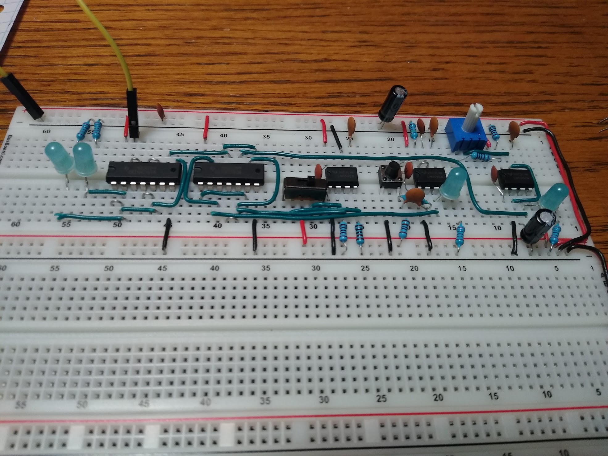
I started where many of us did, the clock module
I started where many of us did, the clock module
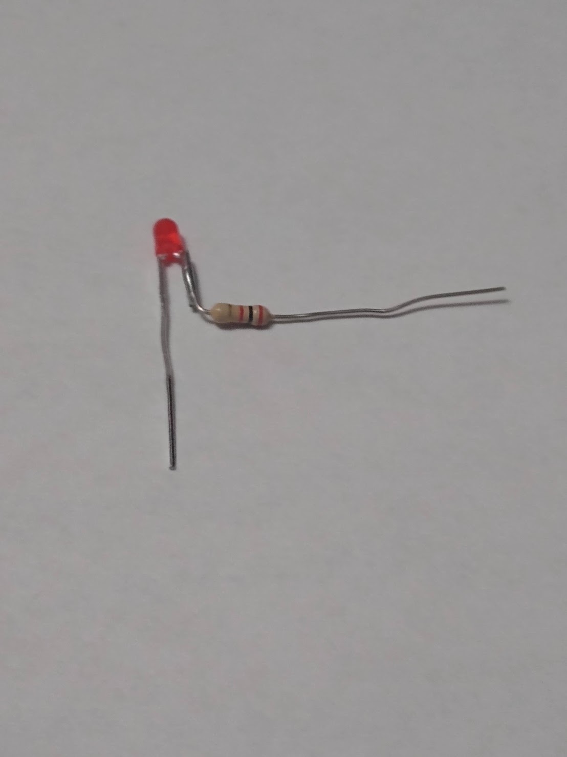
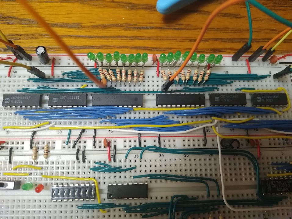
Then the registers, this is how I soldered resistors onto LEDs to save breadboard space
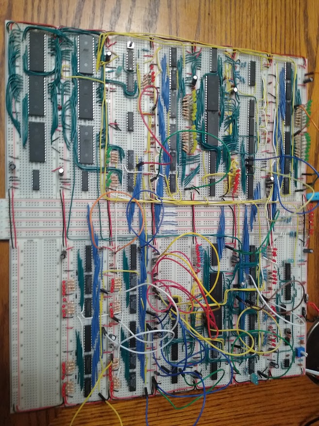
I guess my wiring was still pretty organized
I added Decimal and Hexidecimal modes with an extra address line on the EEPROM
Yay memory
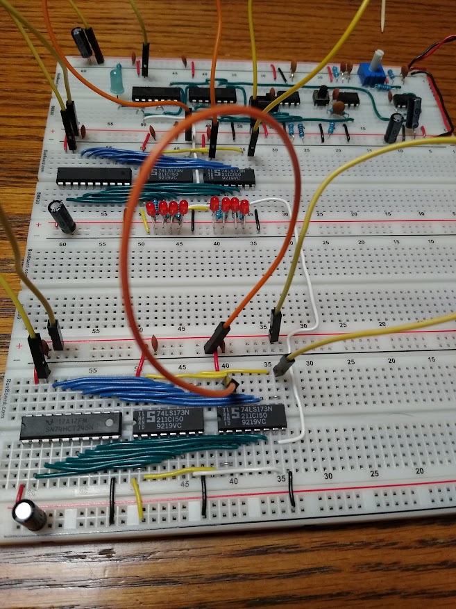
I also added LEDs to view all of the control lines
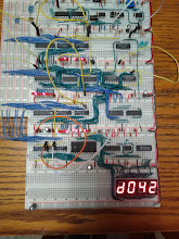
Made a 16 bit program counter, not too much to talk about here
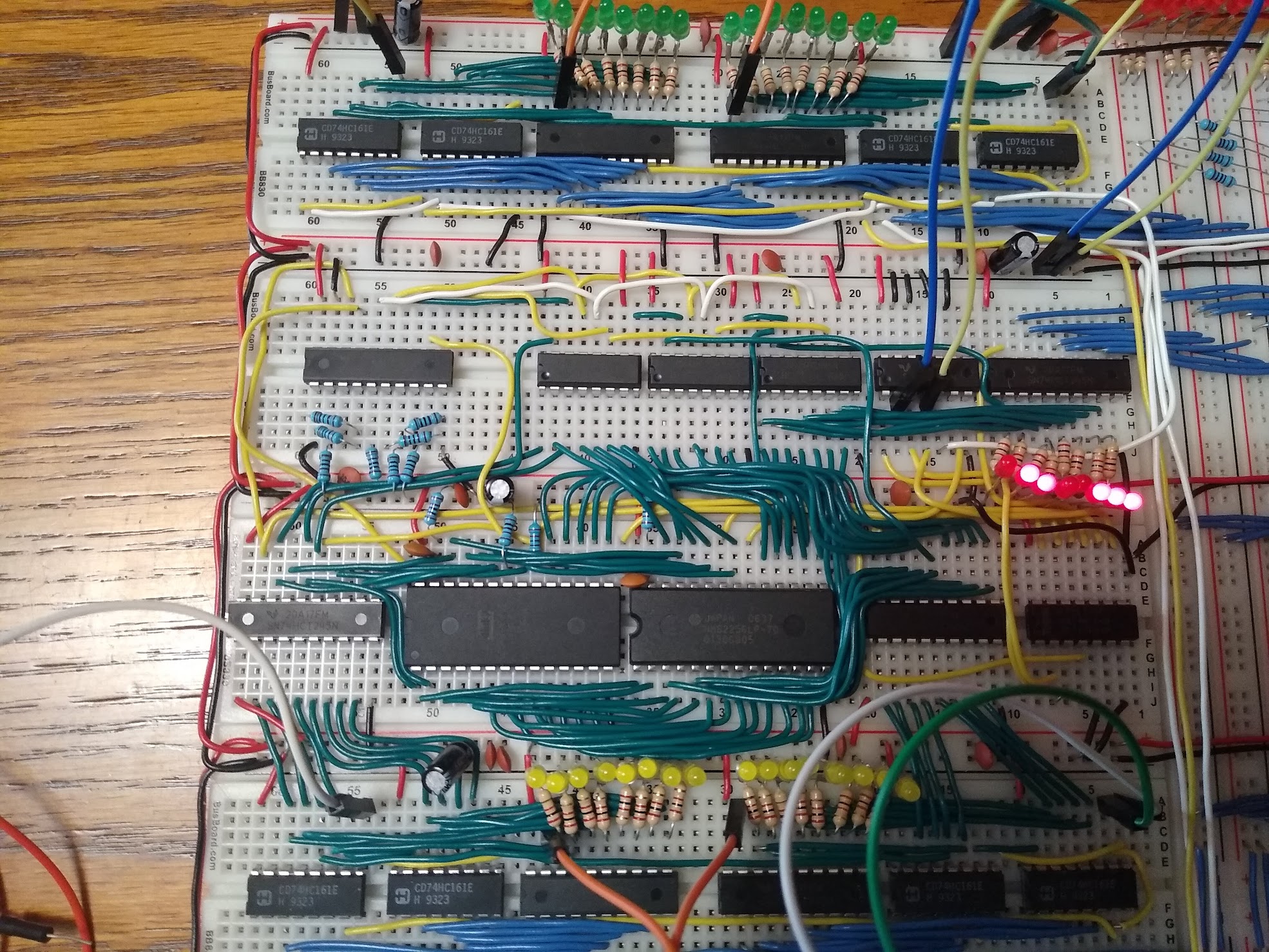
64k memory upgrade, 0x0000 through 0x7fff is ROM, 0x8000 to 0xffff is ram. There is also a setup to connect an arduino that can flash to the rom.
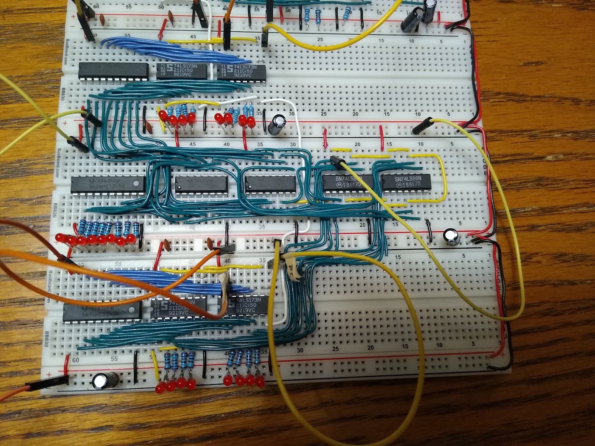
Registers A through D plus an ALU supporting bitwise functions, shifting, adding, subtracting, etc with zero and carry flags for all those functions
Bigger control logic for all the control lines + 4 bit microcode counter. Also two 8-bit output registers, built the same as the A-D registers except they can't output back to the bus
An 8 bit stack pointer (used in the range 0x8100 to 0x81ff in ram), and two 8 bit input registers.
I technically got interrupts working, but theres a lot to improve with the setup, it was a very hacky way to do it. In the video example here the program just increments the A register, and the interrupt just increments the B register, a simple program I made to test the interrupts.
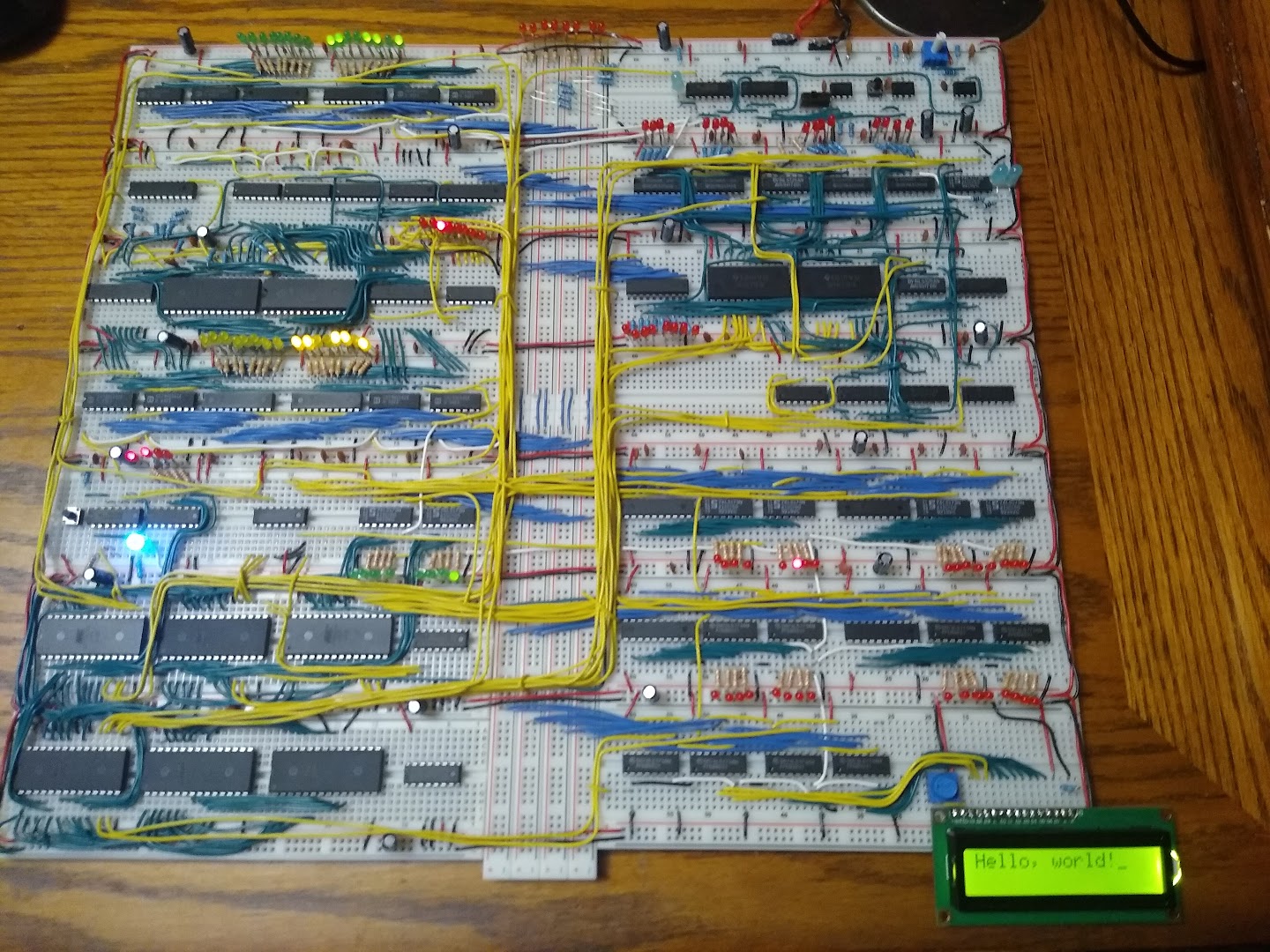
Got a ps2 keyboard interface working!
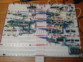
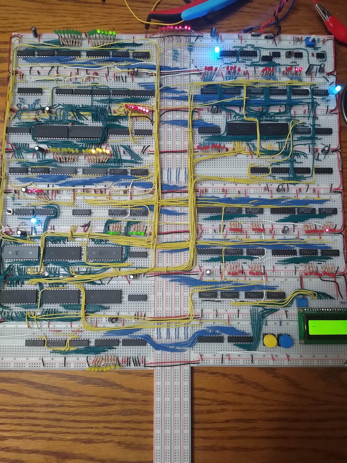
The computer had been in a box for ~2.5 years and I finally got it out and got it running again!
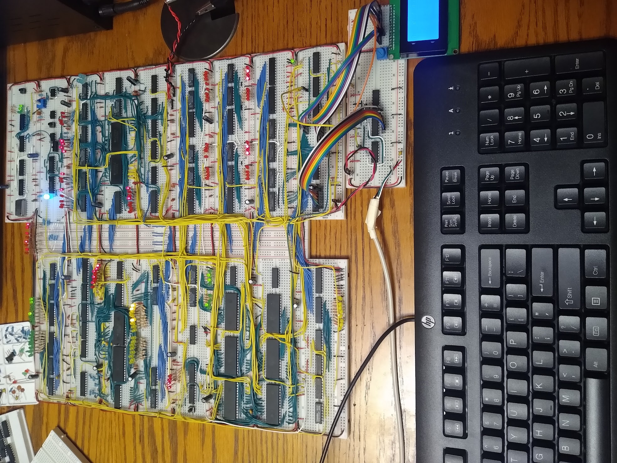
First I need to get the arduino flashing to memory working again, and make the interrupts setup a little less jank, but after that??? Maybe a serial interface? Maybe I finally make some schematics for this thing?
    NOP => 0x00
    HLT => 0x01
    LDA {value: u16} => 0x02 @ value`16
    LDA {value: u16}, B => 0x03 @ value`16
    LDA {value: u16}, C => 0x04 @ value`16
    LDA {value: u16}, D => 0x05 @ value`16
    LDA CD => 0x06
    STA {value: u16} => 0x08 @ value`16
    MVI A, {value} => 0x0A @ value`8
    MVI B, {value} => 0x0B @ value`8
    MVI C, {value} => 0x0C @ value`8
    MVI D, {value} => 0x0D @ value`8
    MOV A, B => 0x0E
    MOV A, C => 0x0F
    MOV A, D => 0x10
    MOV B, A => 0x11
    MOV B, C => 0x12
    MOV B, D => 0x13
    MOV C, A => 0x14
    MOV C, B => 0x15
    MOV C, D => 0x16
    MOV D, A => 0x17
    MOV D, B => 0x18
    MOV D, C => 0x19
    ADD B => 0x1A
    ADD C => 0x1B
    ADD D => 0x1C
    ADI {value} => 0x1D @ value`8
    SUB B => 0x1E
    SUB C => 0x1F
    SUB D => 0x20
    SUI {value} => 0x21 @ value`8
    ANA B => 0x22
    ANA C => 0x23
    ANA D => 0x24
    ANI {value} => 0x25 @ value`8
    ORA B => 0x26
    ORA C => 0x27
    ORA D => 0x28
    ORI {value} => 0x29 @ value`8
    XRA B => 0x2A
    XRA C => 0x2B
    XRA D => 0x2C
    XRI {value} => 0x2D @ value`8
    INR A => 0x2E
    INR B => 0x2F
    INR C => 0x30
    INR D => 0x31
    DCR A => 0x32
    DCR B => 0x33
    DCR C => 0x34
    DCR D => 0x35
    ROR A => 0x36
    ROR B => 0x37
    ROR C => 0x38
    ROR D => 0x39
    ROL A => 0x3A
    ROL B => 0x3B
    ROL C => 0x3C
    ROL D => 0x3D
    RRC A => 0x3E
    RRC B => 0x3F
    RRC C => 0x40
    RRC D => 0x41
    RLC A => 0x42
    RLC B => 0x43
    RLC C => 0x44
    RLC D => 0x45
    JMP {value} => 0x46 @ value`16
    JZ {value} => 0x47 @ value`16
    JNZ {value} => 0x48 @ value`16
    JC {value} => 0x49 @ value`16
    JNC {value} => 0x4A @ value`16
    OUT 1 => 0x4B
    OUT 2 => 0x4C
    JSR {value} => 0x4D @ value`16
    RTS => 0x4E
    IN 1 => 0x4F
    IN 2 => 0x50
    PHA => 0x51
    PHB => 0x52
    PHC => 0x53
    PHD => 0x54
    PLA => 0x55
    PLB => 0x56
    PLC => 0x57
    PLD => 0x58
    STA {value: u16}, B => 0x59 @ value[7:0] @ value[15:8]
    STA {value: u16}, C => 0x60 @ value[7:0] @ value[15:8]
    STA {value: u16}, D => 0x61 @ value[7:0] @ value[15:8]
    PHF => 0x62
    PLF => 0x63